Sio2 Reduction To Si
Sio2 si substrate laser ablation graphene femtosecond Sio2 mhz samples gates Evaluating femtosecond laser ablation of graphene on sio2/si substrate
Silicon Dioxide, SiO2
Nanohub.org Tpr h2 cuo sio2 Dioxide sio2
Sio2 si nanohub resources density dftb silicon binding insulator context functional mosfets modeling thin tight ultra pause previous next
C-v characteristics (1 mhz) for the metal/sio2/si samples with al andH2-tpr profiles of (a) cuo@sio2 and (b) cuo/sio2. Sio2 silicon si substrate oxide thermal wafer wafersSio2 properties water reaction.
Optimized atomic structures of si/sio2 interface structures comprisedSio2 properties and applications Sio2 properties molecule quartz structure atom molecular silicon oxygen gif animated applications form atomsSio2 atomic structures comprised.

Thermal oxide silicon wafer
Sio2 properties and applicationsSilicon dioxide, sio2 .
.


SiO2 Properties and Applications

Thermal Oxide Silicon Wafer | Si+SiO2 Wafer | Thermal Oxide Silicon

H2-TPR profiles of (a) CuO@SiO2 and (b) CuO/SiO2. | Download Scientific
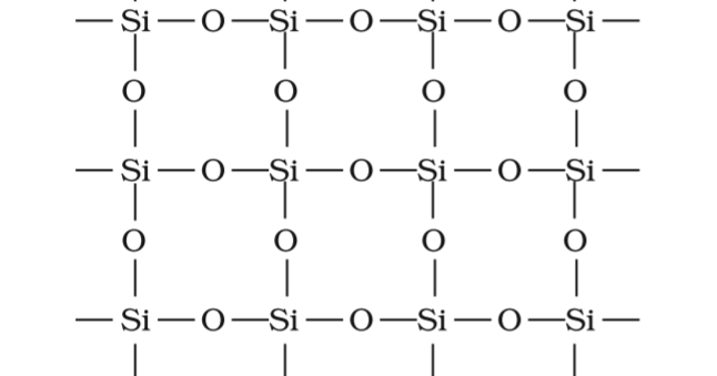
Silicon Dioxide, SiO2

SiO2 Properties and Applications

nanoHUB.org - Resources: Density Functional Tight Binding (DFTB

C-V characteristics (1 MHz) for the metal/SiO2/Si samples with Al and
